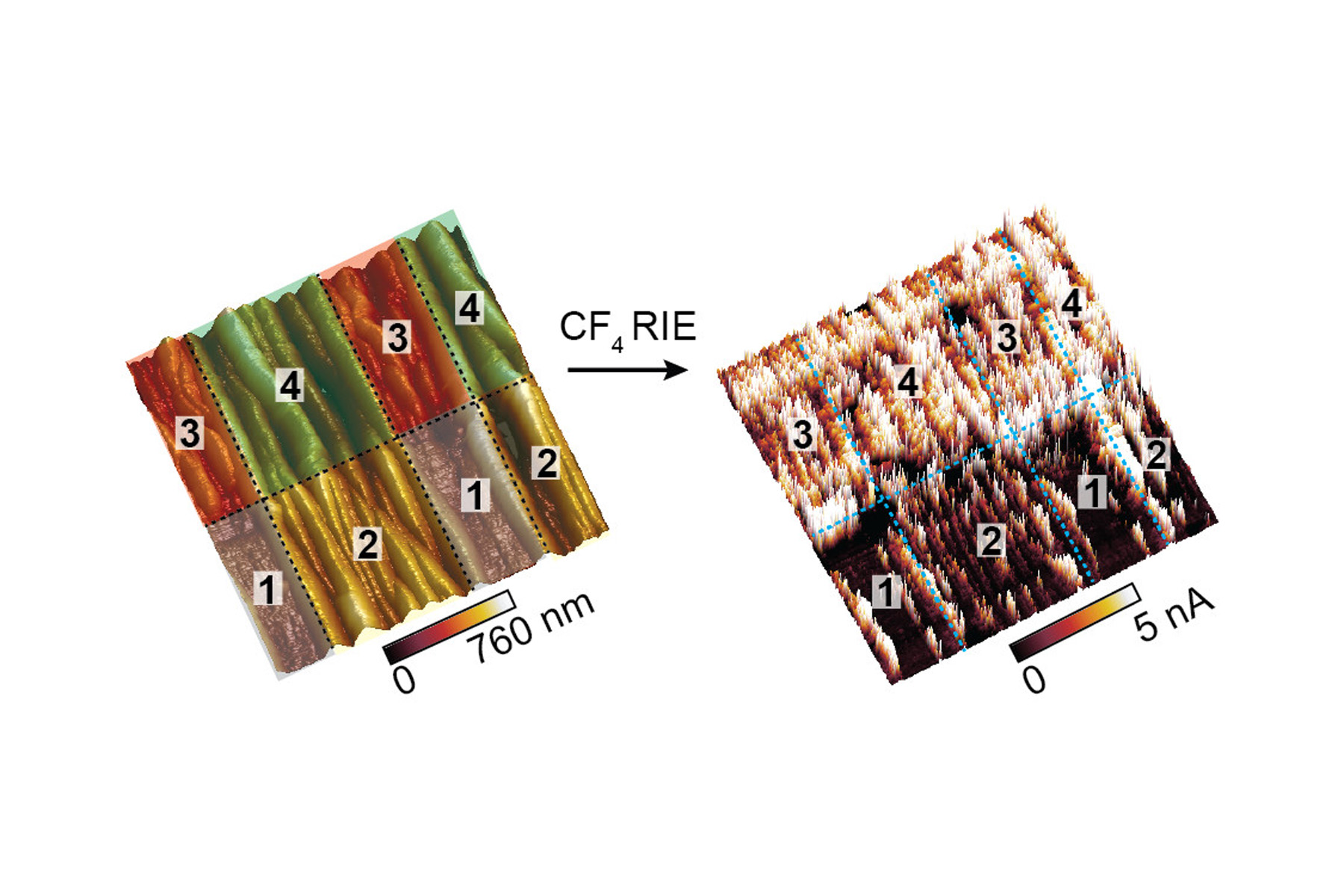
Selectively functionalized graphene can realize spatially defined properties that are highly desirable for atom-thin devices. We developed a scalable approach to realize area-specific properties in graphene using multiscale wrinkles. Patterned areas of graphene nanowrinkles and crumples followed by a single-process plasma reaction resulted in substrates with regions having different fluorination levels. Because the reduction in conductivity scales with the degree of fluorination, the conductivity of the functionalized graphene nanostructures can now be controlled as a function of feature size.