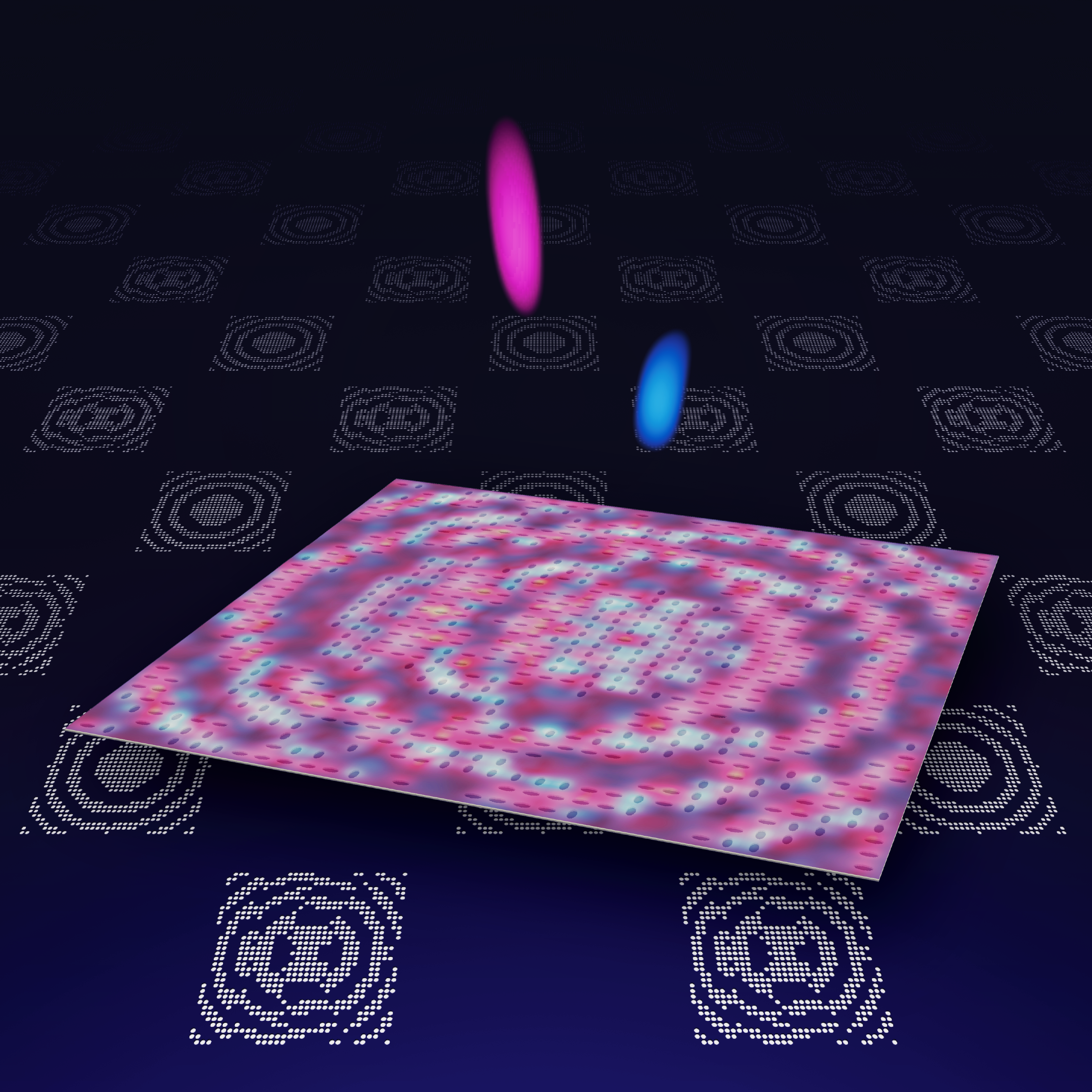
 Plasmonic metasurfaces—structured materials with subwavelength units—are of interest for applications ranging from high resolution imaging to 3D holography. Integrated devices, however, are challenging to achieve because traditional plasmonic materials such as Ag or Au are not compatible with semiconductor processing. Recently, TiN has received attention as an unconventional plasmonic material because of its potential CMOS compatibility as well as exceptional durability required for operation in extreme conditions. However, experimental demonstration of TiN metasurfaces has not been reported due to the difficulties in design and fabrication. We have developed an evolutionary algorithm that can transform plane-wave light into a variety of 3D light profiles. Also, we demonstrated a simple technique to prototype these designs in TiN films by combining ion beam milling and wet etching. By incorporating anisotropic nanohole shapes as building units, TiN lattice lenses could exhibit dynamic tuning of the focal profiles by changing the polarization of incident light. Our optimize-and-prototype platform can contribute to expanding metasurface designs for a wide range of applications requiring unconventional materials.